
AIPE PCB Agent
AIPE PCB Agent is the PCB design agent in the AIPE framework. It turns a converter’s requirements into editable KiCad schematics and board layouts, runs KiCad’s own checks on them and packages the results for engineering review. This page explains the framework it belongs to, its role there, how the agent is organised, and a 5 kW SiC converter it has designed.
The AIPE Framework
AIPE (AI for Power Engineering) is the open engineering ecosystem I am building through AIPE Labs. It treats power-converter design as a coordinated, iterative optimisation process rather than a chain of separate tools. Specialist agents each own one engineering step: electrical sizing, schematic drawing, circuit simulation, device and magnetics selection, thermal and field analysis, mechanical CAD and PCB layout. They exchange explicit inputs, assumptions, results and evidence through a shared Engineering State.
A workflow engine runs these steps as a checkpointed task graph. Results from later stages, such as magnetics or finite-element parameters, feed back into the circuit model, and every result is recorded against a verification gate. Software checks do not replace engineering review, measurement or hardware qualification, which remain separate gates. The first full benchmark is a 10 kW dual-active-bridge converter (800 V → 400 V, 100 kHz).
Role of the PCB Agent
PCB Agent works at the physical-design stage, downstream of AIPE Electrical Design and alongside the CAD Agent, which produces mechanical geometry such as transformers and heat sinks. It takes the converter’s electrical decisions and turns them into boards that an engineer can open, check and revise.
| Interface | Content |
|---|---|
| Inputs | Requirement files: converter specification, insulation-coordination table and stack-ups, component selections with sources, interface pin maps, floorplan and routing inputs |
| Outputs | Native KiCad projects, ERC/DRC and layout-check records, manufacturing exports and review documents |
| Hand-off | AIPE-Workflows re-runs the KiCad ERC and DRC on the generated boards for its CAD/PCB gate; the results then go to human engineering review |
A clean ERC/DRC result is a statement about the generated CAD files under the recorded rule set. It does not establish electrical safety, insulation compliance or manufacturability. The agent interface defines these inputs, outputs and limits.
How the Agent Is Organised
The agent is built around one shared circuit model. The model records every part, pin and net, while schematic drawing and board geometry are generated from it separately. Checks compare the CAD files with the model and feed their findings back to the stage that needs another pass.
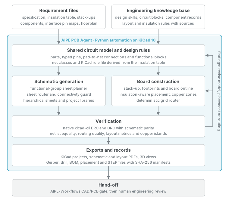
| Part | Responsibility |
|---|---|
| Requirement files | YAML/JSON files hold every number the design uses: ratings, parts, interfaces, insulation distances, stack-ups and floorplan regions. |
| Knowledge base | Design skills, circuit blocks, component records and layout rules, each traced to manufacturer or reference-design sources. |
| Circuit model and rules | Converter-specific Python modules build the part and connection model; net classes and KiCad design rules are derived from the insulation table. |
| Schematic generation | Groups parts by function, draws and routes hierarchical sheets, and refuses to write a sheet whose connectivity differs from the model. |
| Board construction | Sets the stack-up, places parts with insulation-aware spacing, forms copper zones and routes connections with a deterministic grid router. |
| Verification | Runs native kicad-cli ERC and DRC with schematic parity, then checks netlist equality, routing quality, layout metrics and copper islands. |
| Exports and records | Writes editable projects, PDFs, Gerber, drill, BOM, placement and STEP files, with SHA-256 manifests linking each output to its sources. |
The converter-specific modules supply only design data and policies, while the shared tools do the CAD generation and checking. This lets buck, DAB and future converter projects reuse the same operations. The automation architecture and task workflow describe the modules and their acceptance gates.
Example: 5 kW SiC Buck Converter
This example shows a complete task, from the specification to two routed boards. The agent was asked to design a SiC synchronous buck converter; its design requirements specify:
| Parameter | Design value |
|---|---|
| Nominal input voltage | 400 V |
| Output voltage | 200 V |
| Output power | 5 kW |
| Nominal output current | 25 A |
| Switching frequency | 50 kHz |
| Power devices | Wolfspeed SiC MOSFETs |
| Controller | TI TMS320F28335 DSP |
From Requirements to Boards
The task followed the agent’s workflow:
- Requirements and engineering. Values the task left open, such as the input range, cooling and ripple targets, were recorded as labelled assumptions. Calculations and the knowledge base then selected the parts: Wolfspeed C4MS025120K SiC MOSFETs, UCC21710-Q1 isolated gate drivers with UCC14141-Q1 bias modules, a custom 272 µH High Flux toroid and isolated current and voltage sensing.
- Architecture. The agent compared board arrangements and chose two boards: a power board for conversion, gate drive, sensing and protection, and a DSP control board connected through a 2 × 25 mezzanine.
- Schematics and boards. It generated hierarchical schematics, placed the parts with insulation-aware spacing along each board’s isolation barrier, and routed both four-layer boards.
- Checks and outputs. Both boards reached zero native ERC/DRC findings with schematic parity, and the exported netlists matched the circuit model exactly. The task then produced the review package.
Power Board
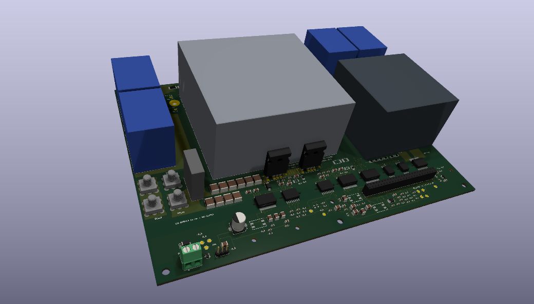
The 240 × 180 mm power board groups the SiC switching stage, isolated gate drivers and bias supplies, DC-link capacitors, output filter, sensing and protection circuitry. The layout separates the high-voltage power path from the low-voltage interface used by the control board.
Control Board
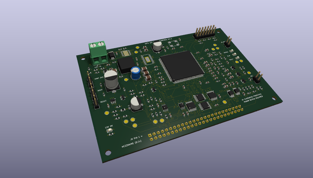
The 120 × 80 mm control board brings together the TMS320F28335 DSP, local supplies, signal conditioning, PWM and protection interfaces, and debug connections. The mezzanine connector stacks it on the power board’s low-voltage strip, keeping the control circuitry on a separate PCB.
Task Outputs
The task produced two editable KiCad board projects and their schematics, together with BOMs, placement files, Gerbers, drill files, STEP models, check reports and hashed manifests. The design is a CAD-complete prototype for review: no board has been fabricated, energised or measured.
A later clean-sheet revision (V3) redesigned the same converter after an independent review, moving the control board beside the power board on a keyed cable and mounting the heavy magnetics on the chassis. The V3 package and the example history link each revision to its design records and review packages.