
GaN Current Capability Test
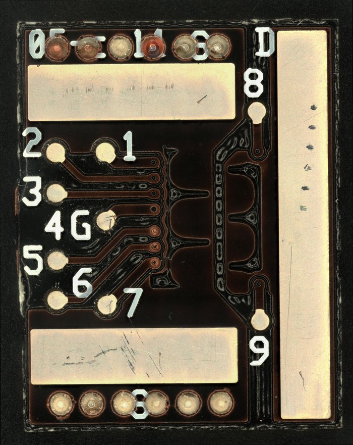
For the P3EP project, the current capability of a packaged GaN power device was tested by stepping its drain current and tracking its junction temperature through a temperature-dependent resistance on the chip. The test uses the same packaged device as the thermal-resistance measurement.
What Limits the Current
A power device’s current rating is set less by the semiconductor than by heat: the conduction loss grows with the square of the current, and the junction temperature rises with that loss through the device’s thermal resistance. The usable current is therefore the current at which the junction reaches its temperature limit in a given package and cooling arrangement. Measuring it directly needs a reliable reading of junction temperature while the device conducts.
Test Method
The device sits in an enclosure with its gate on. A supply steps the drain current, and the on-chip sensing resistance is read alongside it as the junction thermometer.
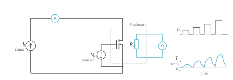
- Calibrate: map the sensing resistance against temperature, with the gate both off and on, because driving the gate shifts the reading.
- Step the current: drive the drain current through a series of increasing steps, each held long enough for the temperature to settle.
- Track the temperature: convert the sensing resistance to junction temperature with the gate-on calibration at each step.
Calibration
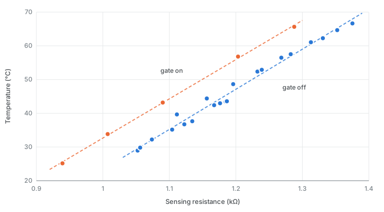
In both gate states, the sensing resistance rises linearly with temperature; across the two, the readings span about 0.94 to 1.38 kΩ over 25 to 67 °C. The gate-on curve is offset from the gate-off curve, so each state needs its own mapping; the gate-on fit, about 116 °C per kΩ, is the one used during the current test. The gate-off data combine two calibration runs.
Stepped Current Test
During the test, the sensing resistance steps up with each increase in drain current and settles at a higher level, then falls back towards its starting value between steps. Over the sequence it rises from about 940 Ω to about 1150 Ω, which the gate-on calibration places at roughly 25 °C and 50 °C.
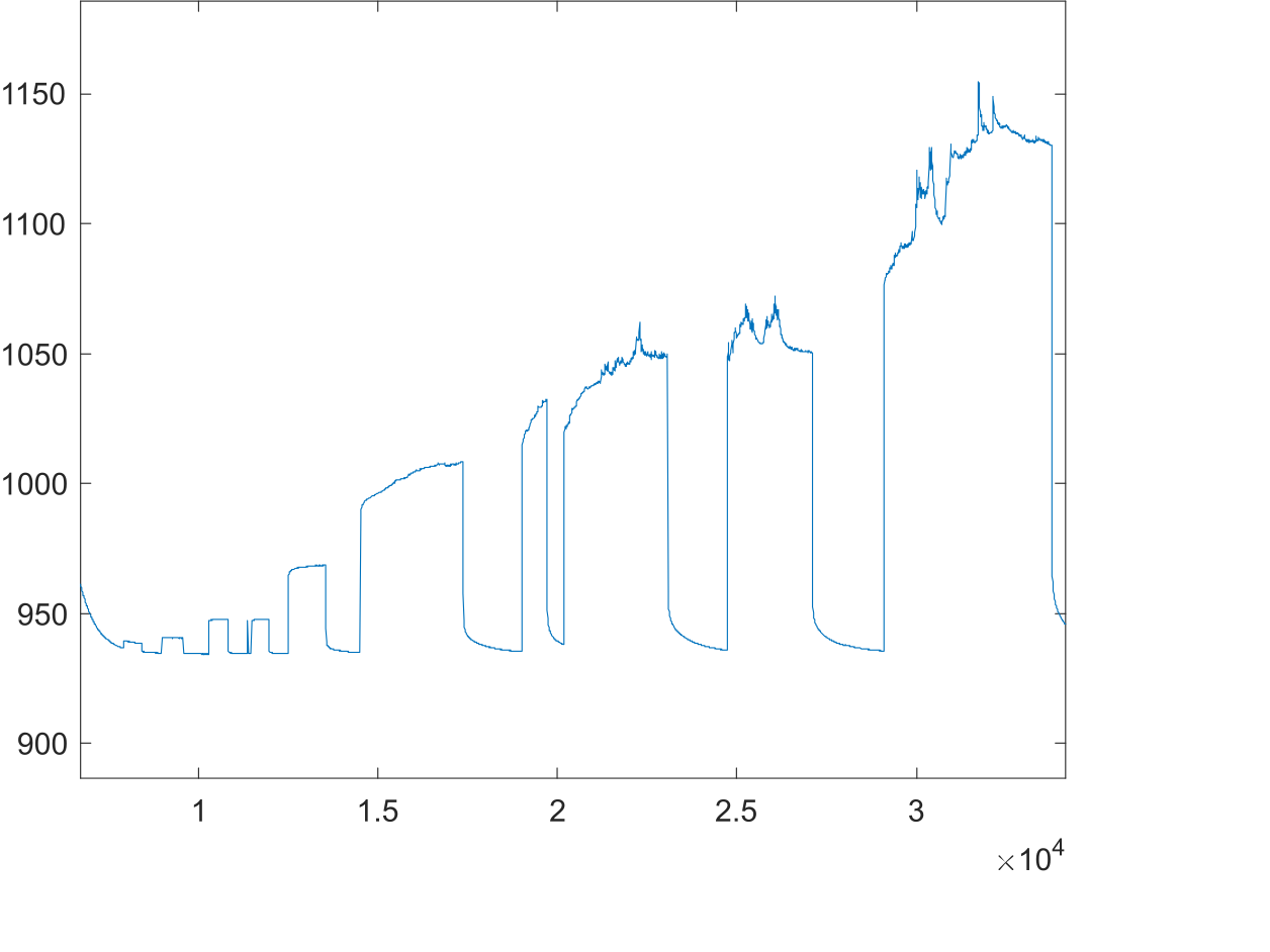
Extending the steps until the junction reaches its limit gives the device’s current capability in this package and cooling arrangement, and the same data show how quickly the junction settles after each step.
Thermal Characterization · Power Device Characterization · Back to Research