
Thermal Characterization
Thermal characterisation determines how heat leaves power devices. For the P3EP project, a thermal-resistance measurement was built for a GaN power device in an embedded package, using a temperature-dependent resistance on the chip as its thermometer; earlier work measured the transient thermal impedance of a SiC MOSFET.
How Thermal Resistance Is Measured
A power device’s junction temperature cannot be measured directly, yet it sets the device’s losses, lifetime and safe operating limits. Thermal characterisation links the power a device dissipates to the temperature rise from its junction to a reference point, such as the case or the cooling plate:
The steady-state thermal resistance Rth describes the heat path once temperatures settle; the transient thermal impedance Zth(t) describes how it builds up. In both cases the device itself serves as the thermometer: a temperature-sensitive electrical parameter is first calibrated against temperature on a controlled plate, then read while the device dissipates power.
Thermal Resistance of a Packaged GaN Device
The device is a GaN power transistor embedded in a compact package, with drain and source pads, a gate pin and numbered sense pins. A resistance on the chip changes with temperature, which provides the junction-temperature reading.
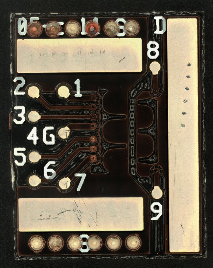
Test Setup
The device is switched on and heated by its own drain current, while the sensing resistance on the chip is read separately as its thermometer and a thermocouple measures the bottom of the package.
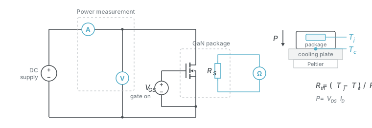
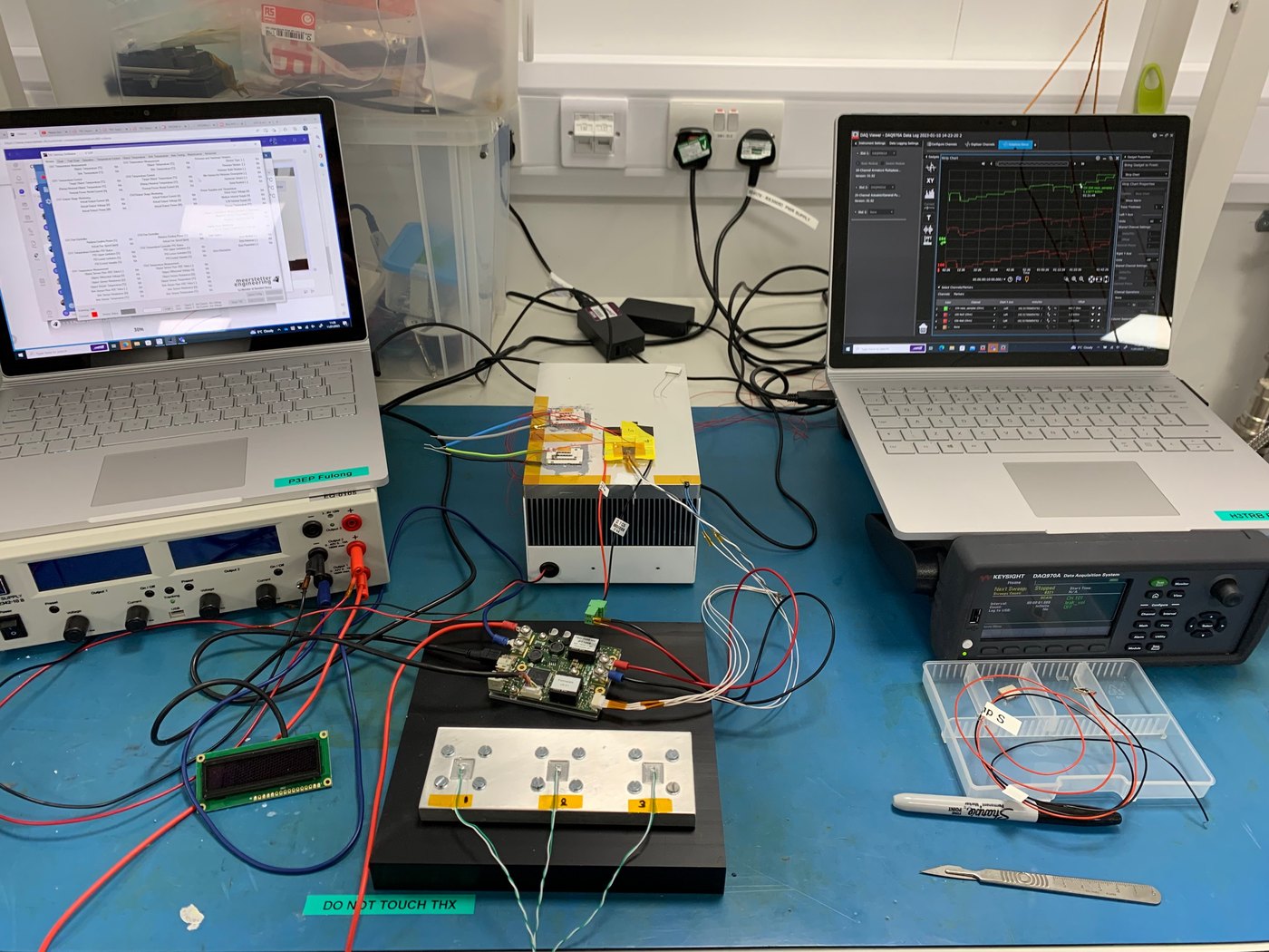
A base cooling plate was designed with six seats, each a 1 mm-deep pocket for the 1.685 mm-thick package, so several devices can be prepared and tested in turn. A Peltier module sets the plate temperature, both for calibration and for temperature cycling. The bench combines a precision power analyser, a dual DC power supply, a data-acquisition unit and a thermocouple logger, recorded from a laptop.

Procedure
- Calibrate: with the device unpowered, step the plate temperature and map the on-chip resistance against temperature.
- Heat: switch the device on and apply power between drain and source to heat the chip.
- Measure: at each power level, record the dissipated power, the junction temperature from the calibrated resistance, and the temperature at the bottom of the package.
- Recalibrate: repeat the calibration to confirm that the mapping has not drifted.
- Evaluate: calculate the thermal resistance from the temperature difference and the power.
Results
The on-chip resistance rises linearly with temperature over the calibration range, giving a mapping of T ≈ 0.107 R − 81.2 °C with R in ohms.
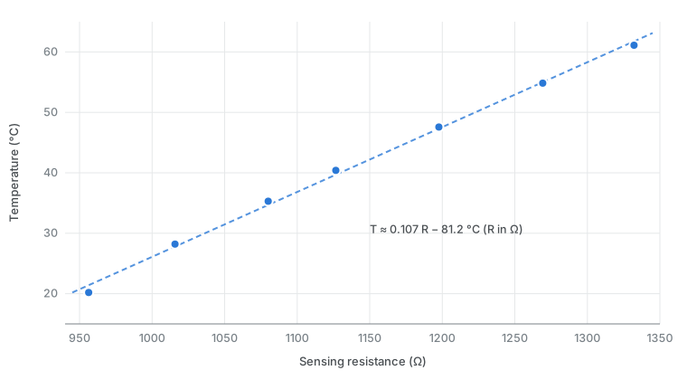
With this mapping, the junction-to-package-bottom thermal resistance of the device came out at about 0.2 K/W. The readings at the lowest power levels scatter widely, because their temperature rise is small compared with the resolution of the measurement.
Transient Thermal Impedance of a SiC MOSFET
The C2M0080120D SiC MOSFET was measured with a PWT2400 power tester, the T3STER transient measurement system and a temperature-controlled cooling circuit. The forward voltage was calibrated at a 10 mA sensing current, the device heated to equilibrium, and its cooling transient recorded. Repeating the measurement with a dry and a greased mounting interface changes only the outer part of the heat path, so comparing the two structure functions locates the junction-to-case boundary. Structure-function analysis then extracts a Cauer thermal network for the device.
The extracted network feeds the thermal branch of the SiC static ANN model and its converter-level temperature estimates. Automation of the measurement workflow continues in the public TIM Automation repository.
GaN Current Capability Test · Double Pulse Test · Power Device Characterization · Back to Research