
SiC Power Devices — Static ANN Modelling
This study, led by the author, developed a data-based model of the C2M0080120D SiC MOSFET for converter loss and temperature calculations. Neural networks fit the device’s conduction, switching-energy and thermal characteristics, so that losses and temperature can be evaluated at any operating point within the data.
Device Characteristics for Loss Models
A converter-level loss model treats each switch as a set of characteristic functions rather than simulating every switching waveform. Three are needed: the conduction voltage as a function of current and junction temperature, the energy lost at each turn-on and turn-off as a function of voltage, current, temperature and gate resistance, and the thermal impedance that turns dissipated power into temperature rise. Circuit simulators with thermal models use the same description while keeping the electrical switching ideal.
These characteristics come as tables from datasheets, manufacturer models and measurements. An artificial neural network (ANN) can learn each table as a continuous function, so the loss model can be evaluated smoothly at any operating point within the data. The model represents characteristic surfaces; it does not resolve the electrical waveform during a switching transition.
Building the ANN Model
Model Branches
The reference data were organised as current–temperature–voltage samples for conduction and as event energies at specified voltage, current and temperature for switching, treating the body diode separately from the MOSFET channel. The public training implementation uses fully connected feedforward networks with ReLU hidden layers and linear outputs:
| Model branch | Inputs | Hidden layers | Output |
|---|---|---|---|
| MOSFET conduction | IDS, Tj | 32 → 32 | VDS |
| Body-diode conduction | ID, Tj | Separate 32 → 32 | VF |
| Turn-on / turn-off energy | I, V, Tj, Rg,on, Rg,off | Shared 32 → 32 | Separate Eon and Eoff heads |
| Thermal response | Time | Separate 64 → 64 | Zth(t) |
Separate conduction networks let the channel and diode characteristics be fitted independently, while the two switching outputs share one hidden representation.
Training
Electrical inputs are standardised with the training-set mean and standard deviation, and the same scaler is saved with the weights for later queries. Training holds out 20% of the electrical samples and minimises the sum of the five branch mean-square errors with the Adam optimiser at a 0.01 learning rate over 2,000 epochs. The hold-out split checks interpolation within the tables.
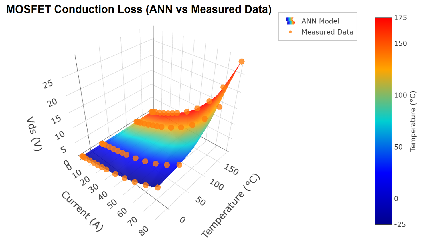
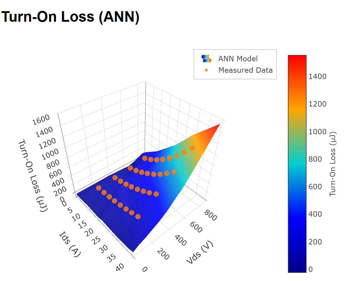
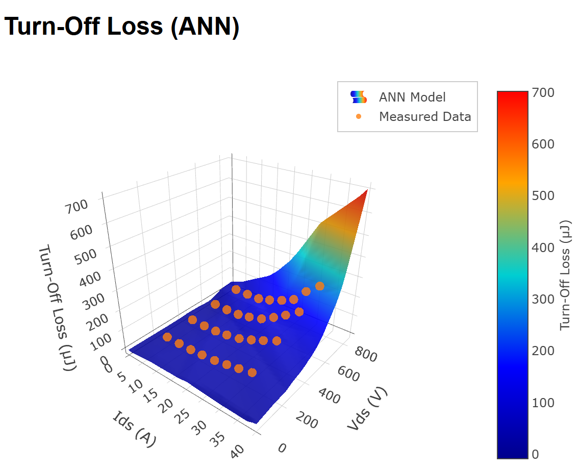
The public implementation extends the gate-resistance dependence with fitted scaling relations; those generated samples extend the data representation and are not independent double-pulse measurements.
Loss Calculation
A Python loss workflow evaluates the fitted functions at the converter operating point. For a buck converter with duty ratio D and switching frequency fsw:
- Conduction: Pcond = VDS(I, Tj) × I × D.
- Switching: Psw = [Eon + Eoff] × fsw.
Thermal Response
An ANN branch fits the transient thermal impedance of the manufacturer’s Cauer model, giving a response function from dissipated power to temperature rise.
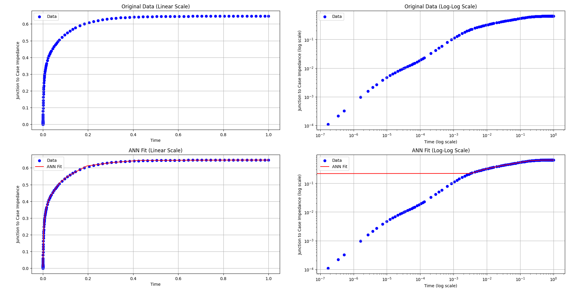
A Cauer network extracted from the device’s own thermal measurement, described under thermal characterization, can replace the manufacturer model in the same role.
Scope of the Model
The model applies within the ranges of its reference data and characterised gate-drive conditions. The networks are unconstrained, so they do not enforce zero-current behaviour or monotonicity outside those ranges. The public training implementation is a reference implementation; its input tables should be reviewed before it is used as a validated C2M0080120D model.
Semiconductor Device Modelling · Double Pulse Test · Converter Design Optimisation · Back to Research