
Double Pulse Test
Double-pulse tests (DPT) measure how power devices switch. This work covers a jointly built DPT platform for SiC MOSFETs with its measurement campaign, and a double-pulse test board designed for GaN devices in the P3EP project.
How Double-Pulse Testing Works
Converter loss models need to know how much energy a power device dissipates each time it switches, across the voltages, currents, temperatures and gate resistances it will meet in operation. A double-pulse test measures this directly under controlled conditions.
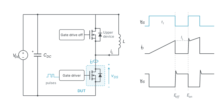
The device under test is the lower device of a half-bridge, supplied from a charged DC-link capacitor bank, with a load inductor across the upper device, which is held off. The first pulse builds current in the inductor to the chosen value,
The DUT then turns off, and the inductor current freewheels through the upper device. The second pulse turns the DUT on again at almost the same current before a final turn-off. Because the inductor holds the current nearly constant over the short gap, both switching events occur at a known voltage and current. Recording the drain voltage and current through these transitions gives the turn-off and turn-on energies:
Static I–V and C–V measurements complement the switching characteristics with the device’s conduction and capacitance characteristics. The same circuit is also used in qualification: the AQG 324 guideline for automotive power modules determines a module’s parasitic stray inductance from a double-pulse turn-off.
SiC MOSFET Double Pulse Test
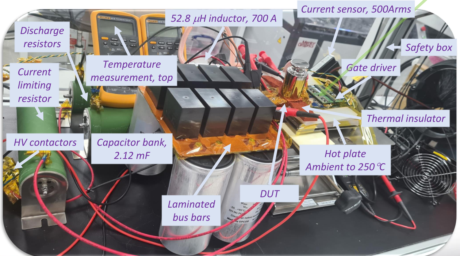
The platform was assembled jointly, with a modified version of the original test board. The rig combines a 2.12 mF capacitor bank and a 52.8 µH load inductor with laminated busbars, a gate driver and a heated device mounting, so that switching conditions can be repeated at controlled temperatures.
The campaign covered more than 450 test points, varying DC-link voltage, load current and gate resistance at 25 °C, 75 °C and 125 °C. Static characteristics were measured with a Keysight B1505A. Acquisition was manual; post-processing was automated. It aligns the voltage and current channels, corrects offsets, integrates instantaneous power over the switching window and extracts current and voltage slew rates and reverse-recovery quantities.
The resulting datasets supply the switching-loss inputs for device modelling. The waveform post-processing is continued in the public DPT Automation repository.
GaN Double Pulse Test
The test principle is the same for GaN devices, but they switch in a few nanoseconds, which turns the test largely into a layout and measurement problem. The parasitic inductance of the power loop, from the capacitors through both devices and back, causes voltage overshoot and ringing at turn-off, so the loop must be kept as small as possible. The probes need enough bandwidth, and short enough ground connections, to capture the edges faithfully. GaN transistors also have no body diode: while the upper device freewheels with its gate off, it conducts in reverse through its own channel.
GaN Double-Pulse Test Board
A half-bridge double-pulse test board, DPT-P3EP V1.0, was designed in October 2024 for the P3EP project’s GaN devices.
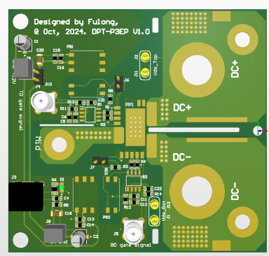
- Power loop: the DC+ and DC− terminals sit on wide copper areas close to the devices, keeping the commutation loop short.
- Load connection: a Mid terminal at the half-bridge midpoint connects the load inductor.
- Gate drive: the top and bottom gate signals arrive on coaxial (SMA) connectors and drive separate gate-drive circuits, each with its own supply module, powered from a 12 V input.
- Measurement: Vds_Top and Vds_Bot pins give access to the drain–source voltage of each device.
Thermal Characterization · Power Device Characterization · Back to Research