
Embedded-Core PCB Current Transformer
This work designed a current transformer whose magnetic core is embedded between PCB layers, with a secondary winding formed by PCB traces and vias, and built a design workbook that sizes it for bandwidth, saturation and trace current. The construction aims at compact, isolated current sensing that can be manufactured repeatably at scale.
How a PCB Current Transformer Works
A current transformer couples the current in a primary conductor into a secondary winding through a magnetic core. The primary conductor passes through the opening in the core, and its changing current induces a secondary current scaled by the turns ratio:
Unlike an air-cored Rogowski coil, the core concentrates the flux and the secondary delivers a current directly into a burden resistor, without an integrator. The core also brings two limits: a current transformer measures changing current only, so its low-frequency response depends on the magnetising inductance, and the core must not saturate in the intended application.
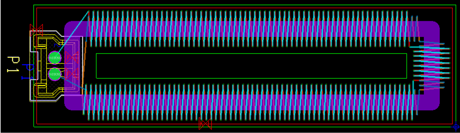
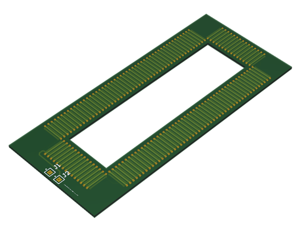
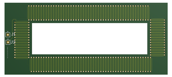
The concept embeds a rectangular ferrite core in the board around a slot for the primary conductor. The secondary turns are routed as traces and vias along both long sides of the core and joined across the far end, with the terminals and protection diodes at the connector end.
Equivalent Circuit and Bandwidth
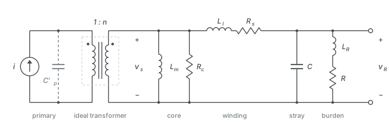
Referred to the secondary, the transformer behaves as an ideal 1 : n transformer loaded by the magnetising inductance Lm and core-loss resistance Rc, followed by the leakage inductance Ll, winding resistance Rs, stray capacitance C and the burden R. The workbook follows the bandwidth model of Kondrath and Kazimierczuk.
The core geometry sets the magnetising inductance and core-loss resistance, with core path length lc, cross-section Ac, permeability μr and ferrite resistivity ρc:
At low frequency, Lm shunts current away from the burden; the lower corner is set by the resistance it sees. At high frequency, the stray capacitance and the leakage inductance each add a pole:
The usable bandwidth is fH − fL. More turns or a higher-permeability core lower fL; a smaller burden or less stray capacitance raises fH.
Design Calculation
The workbook takes the core, winding and burden as inputs, then returns the corner frequencies, the saturation margin and the minimum trace width. For a 200 A primary current through a single primary turn:
| Input | Value |
|---|---|
| Turns, primary and secondary | 1 and 100, giving 2 A secondary current |
| Ferrite core | 20 mm path length, 6 mm × 2 mm cross-section, μr = 125, ρc = 10 Ω·m |
| Secondary winding | 2 oz (70 µm) copper, 0.4 mm traces, 5 mm per turn, 1 m in total |
| Burden | 10 Ω, with 0.1 µH series inductance |
| Parasitics | 0.126 µH leakage inductance, 0.81 nF stray capacitance |
| Result | Value |
|---|---|
| Magnetising inductance Lm | 0.942 mH |
| Core-loss resistance Rc | 16.7 kΩ |
| Winding resistance Rs | 0.62 Ω |
| Lower corner fL | 1.8 kHz |
| Upper corner fH | 19.7 MHz, set by the burden and stray capacitance; the leakage pole lies near 21 GHz |
| Bandwidth | about 19.7 MHz |
| Saturation current, secondary | 7.2 A, against 2 A in operation |
| Minimum trace width for 2 A at 10 °C rise | 0.39 mm, met by the 0.4 mm traces |
| Burden dissipation at 2 A | 40 W |
These are design estimates, not measured ratings of a finished sensor. The last line shows the main trade-off at this current: a 10 Ω burden carrying the full 2 A must dissipate 40 W, so a lower burden or more secondary turns would be needed for a practical sensor.
Board Design
From the concept, the board was designed with the secondary winding distributed around the central aperture, so the magnetic circuit and winding form one compact, galvanically isolated assembly.
The design files are available in the PCB current transformer repository.