
Solid-State Transformers
The solid-state transformer (SST) work has two parts. For the ASSIST project, a review covered SST technology: high-voltage semiconductor devices, converter configurations, smart-grid functions, reported prototypes and applications. Later, in collaboration with Cardiff University, a three-stage SST was designed in simulation, with a focus on its isolated dual-active-bridge (DAB) stage.
What a Solid-State Transformer Is
A solid-state transformer replaces a bulky line-frequency transformer with power-electronic conversion stages around a compact medium-frequency isolation transformer. Raising the isolation frequency shrinks the transformer, and because the conversion is actively controlled, an SST can also regulate voltage, control active and reactive power, isolate faults, and provide DC ports for renewable generation, storage and DC microgrids. Its feasibility at medium voltage depends strongly on high-voltage semiconductors: the review followed SiC MOSFETs of 10 kV and above in research, against commercial devices that were then mostly SiC modules up to 1.7 kV and silicon IGBTs at 3.3 to 6.5 kV.
Single-, Two- and Three-Stage SSTs
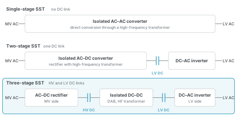
SSTs fall into three configurations, distinguished by how many DC links they have.
| Configuration | Structure | Strengths | Limitations |
|---|---|---|---|
| Single-stage | Direct AC–AC conversion through a high-frequency transformer, with no DC link | Fewest components and conversion stages, so potentially the highest efficiency and reliability | No DC link, so no reactive power support or decoupling between the grids; filtering and control are demanding |
| Two-stage | An isolated AC–DC stage and a DC–AC stage around one DC link, on the high- or the low-voltage side | The DC link enables reactive power compensation, voltage-sag ride-through, fault isolation and DC-link protection | More switching devices, higher losses and ripple current, and harder to build modularly |
| Three-stage | An AC–DC rectifier, an isolated DC–DC stage and a DC–AC inverter, with DC links on both sides | Independent control of each side, fault isolation and ride-through, reactive power support, and HV and LV DC ports for renewables and storage | The most semiconductor stages, so lower efficiency and more components to keep reliable |
The three-stage configuration offers the most complete set of grid functions, including voltage regulation, current limiting, protection and power-factor control, and its two DC links can be brought out as ports for storage, renewables and DC microgrids. This is why most recent research prototypes in the review used it, and why it was chosen for the design. The review also covered the applications that motivate SSTs, from data centres and fast EV charging to DC microgrids, ships and offshore wind.
The Three-Stage SST
A three-stage SST for medium-voltage to low-voltage distribution has three power stages, each with its own control:
- MV-side rectifier. A cascaded H-bridge, modular multilevel or three-level neutral-point-clamped (NPC) rectifier connects to the medium-voltage grid. It regulates the HV DC link and controls the active and reactive power drawn from the grid, using grid synchronisation, current control and DC-link voltage control. An NPC stage must also keep its two DC-link capacitors balanced, by adjusting how long it uses redundant switching states.
- Isolated DC–DC stage. Dual active bridges provide galvanic isolation and bidirectional power transfer between the DC links, often with their secondaries feeding a common LV DC bus. An outer loop on the LV DC voltage sets the phase shift that controls their power.
- LV-side inverter. A three-phase inverter, usually grid-forming, sets the low-voltage magnitude and frequency.
A supervisory layer coordinates the three stages through start-up, shutdown and faults. The design work concentrated on the middle stage.
Designing the DAB Stage
How the DAB Works
A DAB connects two full bridges, each across its own DC link, through a series inductance Ltot (the transformer leakage plus any added inductor) and an n : 1 high-frequency transformer. The transformer provides galvanic isolation and scales the voltage; the inductance is where power is transferred.
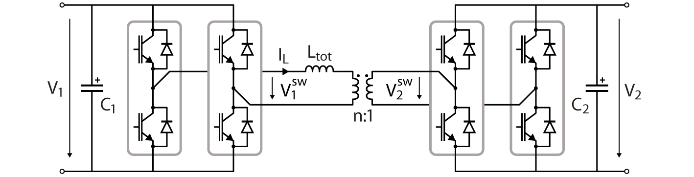
Each bridge applies a square-wave voltage to its side of the transformer. Under phase-shift modulation, both bridges run at 50% duty at the switching frequency fsw, and the shift ϕ between them, as a fraction of the switching period, places a voltage across the inductance and so sets the power. The bridge that leads delivers power, so the same circuit transfers power in either direction, and the inductor current naturally discharges the switch capacitances before each turn-on, giving zero-voltage switching over a wide load range.
For a lossless DAB with DC voltages V1 and V2 and turns ratio n, the transferred power is
positive ϕ sending power from the primary to the secondary and negative ϕ reversing it. Power peaks at ϕ = 0.25.
Choosing the Series Inductance
The series inductance is the central design choice: it sets the power capability, the soft-switching range and how finely the controller can adjust power. Three limits bound it. Zero-voltage switching needs enough stored energy to charge and discharge the switches’ output capacitance Coss in the dead time; the digital controller can change ϕ only in steps of fswΔTPWM, and each step must not change the power by more than a tolerable amount at minimum load; and the inductance must still let the converter reach full power:
For the 15 kW stage, with operation down to 7.5 kW, the ZVS limit was negligible. The control-resolution limit set the lower bound at about 28 µH, keeping each phase step below about 375 W at 7.5 kW, and full power set the upper bound at about 1.1 mH.

A value of 250 µH was selected, made up of about 10 µH of transformer leakage and 240 µH of external inductance. The design model predicts:
| At 15 kW with Ltot = 250 µH | Predicted value |
|---|---|
| Phase shift | ϕ ≈ 0.030, about 1.5 µs |
| Power resolution | about 37 W per phase step |
| RMS current, primary / secondary | 9.73 A / 14.60 A |
| Conduction loss, primary / secondary bridge | 15.16 W / 8.95 W, 24.1 W in total |
| Efficiency, conduction losses only | about 99.84% |
| Zero-voltage switching | down to about 32 W |
These are predictions from the design model in simulation, not measurements; the efficiency counts conduction loss only.
Modulation Options
Phase-shift modulation is not the only way to drive a DAB. Using three-level bridge voltages adds degrees of freedom:
| Modulation | How it works | Trade-off |
|---|---|---|
| Phase shift | Both bridges at 50% duty; power set by the phase shift alone | Simplest control and a wide operating range; the usual choice for SSTs |
| Triangular | Three-level voltages timed so the secondary switches at zero current | Lower switching loss and current stress, but less power, and none when V1 = nV2 |
| Trapezoidal | Extends triangular modulation to zero-current switching on both bridges | More power than triangular with favourable switching, at the cost of more complex control |
In practice, phase-shift modulation combined with a well-chosen inductance and outer-loop control gives stable, efficient operation across a wide range, which is why it was adopted here.
Design and simulation references are collected in the solid-state transformer repository.
Isolated Converters · Power Device Characterization · Back to Research