
Bidirectional Buck–Boost Converter
A modular bidirectional half-bridge converter was developed as the building block of the low-voltage DC microgrid testbeds, connecting battery banks and other sources to the common DC bus with local DSP control.
Bidirectional Power Flow with One Half Bridge
A battery in a DC microgrid must both supply the bus and be charged from it. A half-bridge converter with an inductor on its low-voltage side does both: operating as a Boost converter, it delivers stored energy from the lower-voltage battery to the higher-voltage bus; operating as a Buck converter, the same switches and inductor charge the battery from the bus. The direction of current follows the control, so one converter serves as a two-way interface.
Power Stage and Control Design
The power stage combines the inductor, the two switching devices and the input and output capacitors. Voltage and current transducers feed conditioned measurements to the control board, and isolated gate drives apply its switching commands. A TMS320F28335 DSP runs the local control and operating logic.
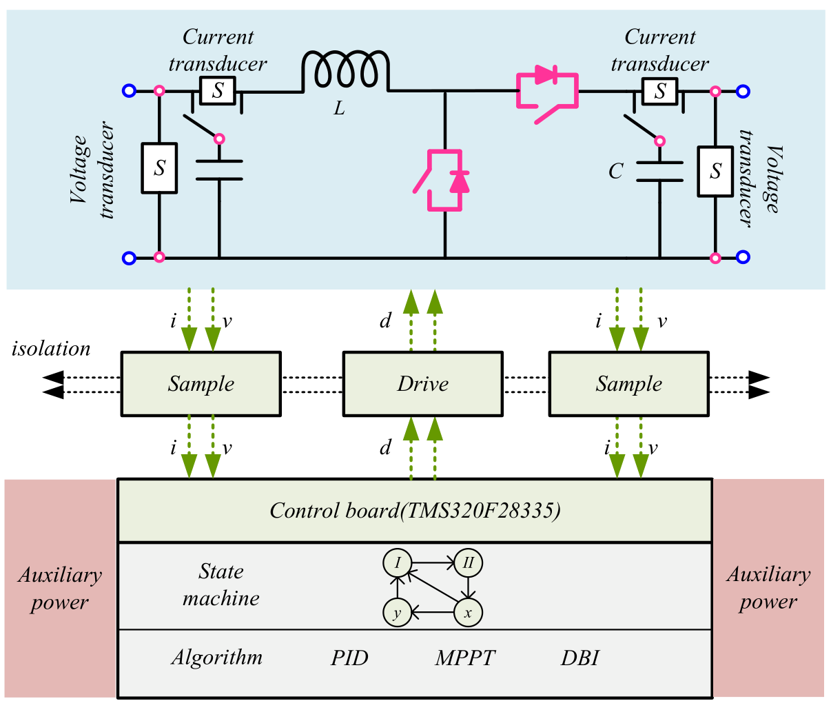
Depending on the source it connects, the controller implements voltage or current regulation, battery charging, PV maximum-power-point tracking and DC bus signalling. The same modular interface can therefore connect a battery bank, a PV source or a grid emulator.
Prototype and PCB Design
Each converter is built as a power board and a control board, galvanically isolated from each other. The power board carries the main power circuit, the MOSFET gate drivers with their own isolated supplies, and isolated voltage and current transducers followed by analogue differential-amplifier and buffer stages. A switch between the output capacitor and the current transducer lets the transducer measure the current on either side of the capacitor, keeping the board ready for connecting several microgrids. The control board carries the microcontroller card and the auxiliary power supplies.
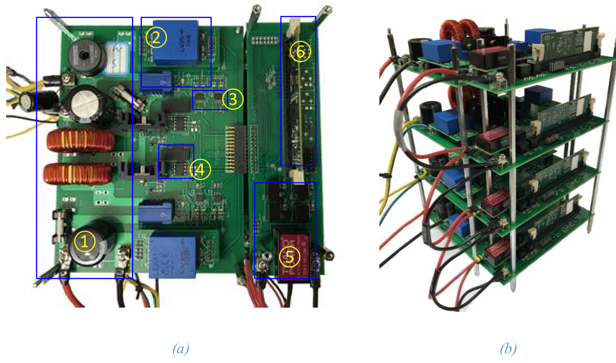
| Area | Function | Area | Function |
|---|---|---|---|
| 1 | Main power circuit | 4 | MOSFET driver circuit |
| 2 | Voltage and current transducers | 5 | Auxiliary power module |
| 3 | Analogue signal processing | 6 | Microcontroller card |
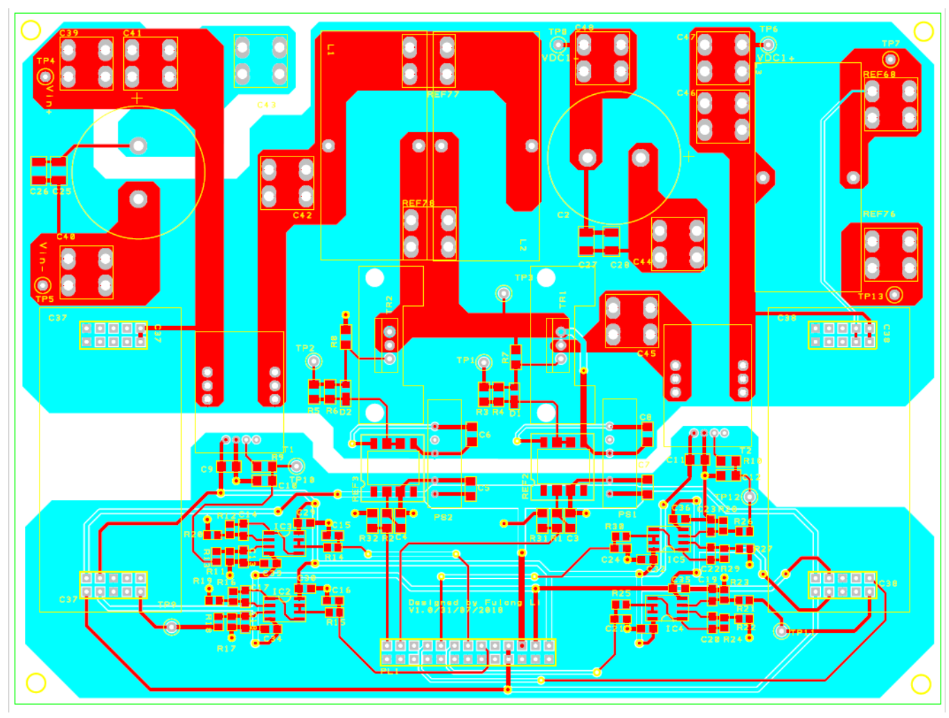
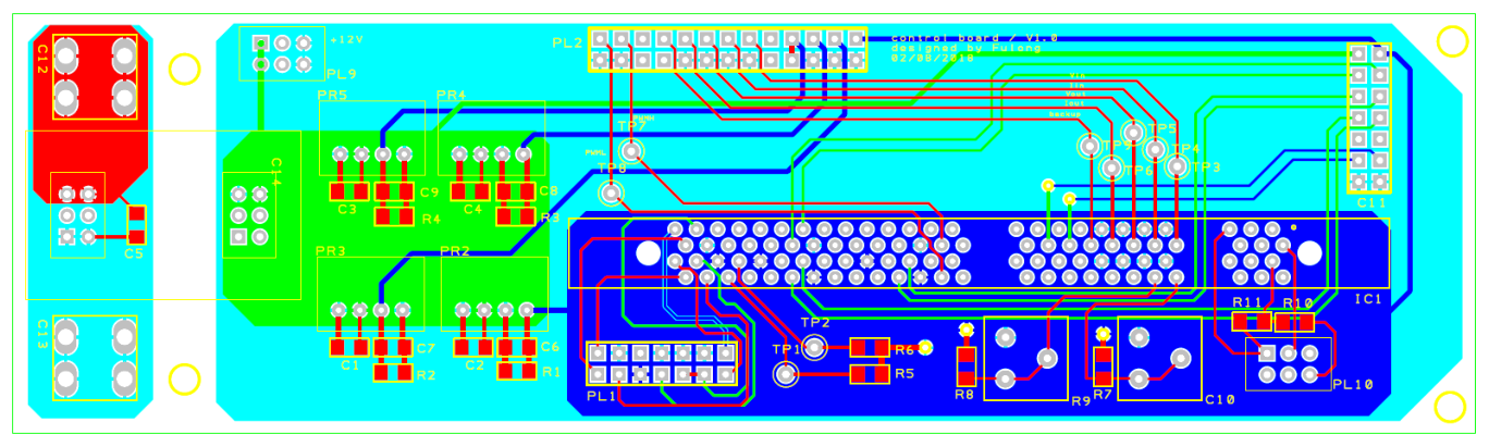
Ratings and System Use
The Aston PhD prototype is rated at 250 W per interface, with a 240 µH inductor and 470 µF input and output capacitors. Each battery bank uses two 12 V batteries in series. Four interfaces connect the grid emulator, two battery banks and the PV emulator, which operates in the Boost direction. A later version, documented with the Loughborough test bench, is rated at 500 W per converter.
These converters carried the stability, droop and supervisory-control studies of the DC microgrid research.
PhD thesis, Chapter 3 and Appendix A1 · Aston testbed · Loughborough testbed · Non-isolated converters